Rc circuit model for a gate driver with mosfet output stage and power device as a capacitor.
Mosfet gate driver power dissipation.
Switch mosfet gate losses can be caused by the energy required to charge the mosfet gate.
These are both turn on and turn off gate losses.
If power dissipated on a current sense resistor is too high or it is difficult to find current sense resistor with the appropriate value for current limiting an additional comparator can be used as shown on figure 2b.
Therefore the maximum usable gate drive power is always derived from setups with non oscillating driver output current.
Gate drive losses are frequency dependent and are also a func tion of the gate capacitance of the.
R ds on also directly affects power dissipation internal to the driver.
Driver output current oscillations may lead to additional power dissipation in the gate driver unit due to clamping effects and non linear behaviour of the output stages and controlling circuitry.
It is a power amplifier that accepts a low power input from a controller ic and produces the appropriate high current gate drive for a power mosfet.
The output drivers feature a high pulse current buffer stage designed for minimum driver cross conduction.
The floating channel can be used to drive an n channel power mosfet or igbt in the high side configuration which operates from 10 to 600 v.
Decades of application expertise and technology development at both infineon and international rectifier have produced a portfolio of gate driver ics for use with silicon and wide bandgap power devices such as mosfets discrete igbts igbt modules sic mosfets and gan hemts we offer excellent product families of galvanic isolated gate drivers automotive qualifies gate drivers 200 v 500 700.
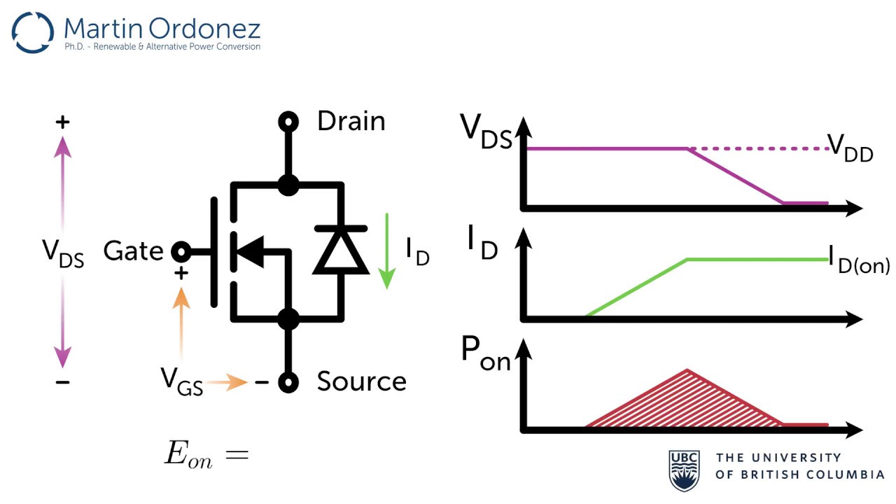
Power dissipation during on time.
Most of the power is in the mosfet gate driver.
The logic input is compatible with standard cmos or lsttl output down to 3 3 v logic.
A gate driver is used when a pulse width.
The rest of this post will show the calculations on where power is dissipated in the mosfet and compare the two designs.
That is the q g tot at the gate voltage of the circuit.
The mosfet s own.
Increase the gate driver current lowering switching losses.
For a specific drive current the lower value of r ds on allows higher r ext to be used.
That allows direct connection of the mcu to the gate driver in case of mosfet as gate driver load with.